Toshiba Unveils 100V N-Channel MOSFET for Superior Power Efficiency
Pune, India | September 29, 2025
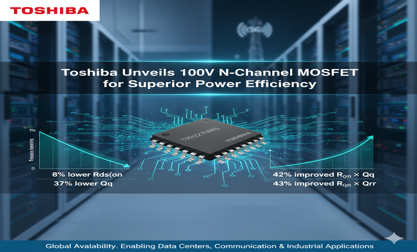
Toshiba Electronic Devices & Storage Corporation recently introduced its new 100V N-channel power MOSFET, named TPH2R70AR5. Built on the company’s advanced U-MOS11-H process, this high-efficiency device is designed to boost power conversion in switched-mode power supplies (SMPS). These SMPS units are essential for data centers, communication infrastructure, and various industrial applications. The product is now available globally, with shipments already underway.
The TPH2R70AR5 demonstrates considerable efficiency gains over previous-generation MOSFETs. Specifically, it delivers approximately 8% lower drain-source on-resistance (Rₒₙ), which reduces conduction losses. Additionally, the device features a 37% reduction in total gate charge (Qg), further minimizing switching losses. Combined, these improvements lower the Rₒₙ × Qg figure of merit by 42%, highlighting the MOSFET’s enhanced energy efficiency and switching performance. Therefore, it provides a direct advantage in systems that require precise energy control and minimal power loss.
Moreover, Toshiba has integrated its proprietary lifetime control technology into the device. This innovation reduces the reverse recovery charge (Qrr) of the body diode by 38%, which is vital for high-speed switching performance. The improvement results in a 43% enhancement in the Rₒₙ × Qrr figure of merit. These figures translate to lower diode losses and improved thermal stability, particularly in circuits requiring rapid switching capabilities. Hence, designers working on high-frequency applications will find this improvement significantly valuable.
Notably, the TPH2R70AR5 is housed in the SOP Advance (N) package. This compact and thermally efficient form factor provides excellent heat dissipation. At the same time, it maintains compatibility with widely used mounting footprints. Therefore, engineers can integrate the new device into existing circuit designs without substantial changes, making it a highly adaptable solution for modern power systems. This packaging advantage simplifies upgrades and system optimization across various platforms.
To ensure smooth integration into existing workflows, Toshiba offers simulation models alongside the new MOSFET. These include the G0 SPICE model, which supports quick circuit prototyping, and the G2 SPICE model, designed for high-accuracy simulations. These tools are especially helpful for evaluating switching behavior under diverse load conditions. As a result, developers can accelerate design processes and improve overall system reliability through thorough simulation and testing.
Toshiba has highlighted that the TPH2R70AR5 delivers best-in-class trade-offs between performance metrics. Consequently, the MOSFET is ideally suited for use in high-efficiency power conversion systems. This includes mission-critical environments such as data centers and 5G base stations, where power efficiency directly affects operational costs and system longevity. By reducing power loss and thermal stress, the device supports long-term reliability and cost-effective operation.
As industries move toward energy-efficient and environmentally sustainable technologies, demand for low-loss semiconductors continues to rise. Recognizing this trend, Toshiba’s development of the U-MOS11-H platform marks a strategic step. It aligns technical innovation with global sustainability goals, enabling reduced energy waste without sacrificing performance. In this way, the new MOSFET supports green energy initiatives across multiple sectors.
Looking ahead, Toshiba plans to expand its range of low-loss MOSFETs, all based on the U-MOS11-H platform. This expansion will include devices across additional voltage classes to meet broader market needs. Simultaneously, the company remains focused on delivering robust design support, allowing engineers to develop optimized power systems more efficiently. These efforts underline Toshiba’s long-term strategy in advancing power device technology.
In conclusion, Toshiba’s TPH2R70AR5 delivers major advancements in power MOSFET performance, offering lower resistance, reduced switching loss, and improved diode behavior. Encased in a thermally efficient and compact package, it is easy to integrate and highly effective in a wide range of power conversion systems. These innovations reflect Toshiba’s strong commitment to pushing the boundaries of power efficiency, thermal performance, and practical design.
With this launch, Toshiba reinforces its leadership in the global semiconductor market, supporting energy efficiency and technological progress in critical electronics infrastructure.